

1 /
1
Wafer Inspection and Metrology
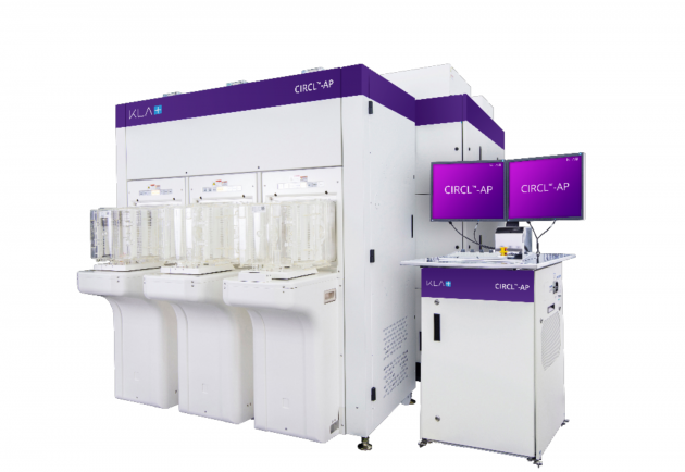
CIRCL™-AP
CIRCL™-AP
Description:
All-Surface Wafer Defect Inspection, Metrology and Review Cluster System
CIRCL™-AP is a cluster tool with multiple modules, covering all-surface inspection, metrology and review at high throughput for efficient advanced wafer-level packaging (AWLP) process control. The CIRCL-AP tool is utilized for multiple AWLP applications requiring high sensitivity including 2.5D/3D integration, wafer-level chip scale packaging (WLCSP) and fan-out wafer-level packaging (FOWLP). With support for bonded, thinned and warped substrates, CIRCL-AP provides production-proven process control and monitoring strategies for Cu-pillars, bumps, through silicon vias (TSVs), redistribution layer (RDL) and other packaging process flows.
Applications:
Process monitor, Outgoing Quality Control (OQC), Tool monitor, Backside monitor, Edge yield monitor, Process tool qualification.
More......