

1 /
1
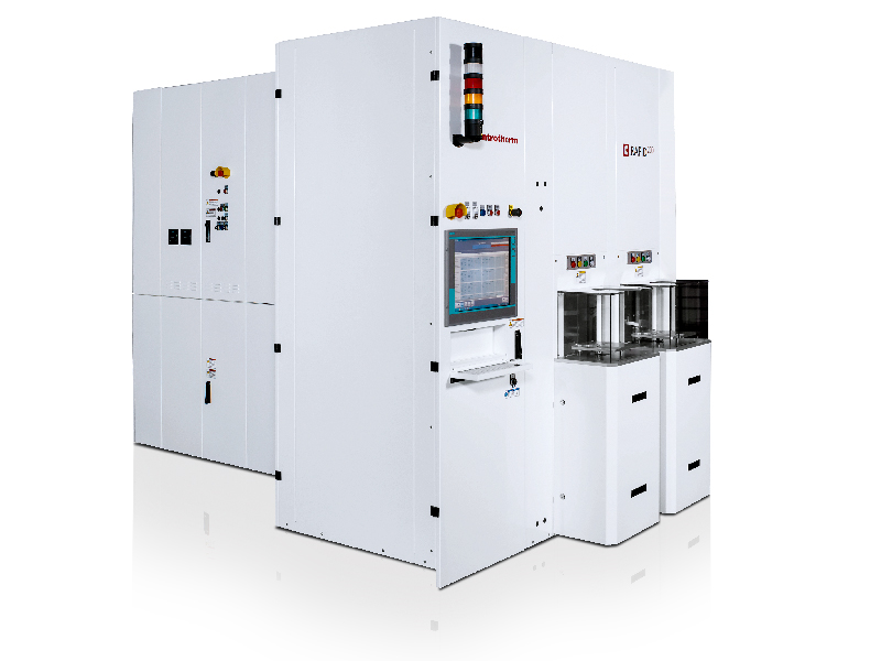
Rapid Thermal Processing System(RTP)
c.RAPID 200
c.RAPID 200
商品簡述:
c.RAPID 200 is a flexible, automatic Rapid Thermal Processing (RTP) system for providing uniform, controlled heating to silicon, germanium and compound semiconductor wafers and pieces under inert or reactive process ambients. centrotherm brings precise temperature and ambient control as well as automatic or semi-automatic wafer handling to small wafer sizes at a reasonable cost.
c.RAPID 200 provides optional vacuum operation and a well-controlled gas management and covers a wide range of heating conditions from 200 to 1200°C within the time range of seconds to a few minutes. The advanced pyrometer-based temperature control enables outstanding thermal accuracy and repeatability.
The modular design allows various configurations for development, small scale pilot production through high volume manufacturing with the same process chamber and process recipes.
Applications :
Rapid Thermal Annealing (RTA)
Ion implant annealing
Contact annealing / metallization annealing
Source/drain anneal
Barrier metal anneal
Further RTA applications
Rapid Thermal Oxidation (RTO)
Silicide formation (Ti, Co, Ni, Pt, etc.)
PSG reflow
Dopant activation
Further RTP applications
Substrates : Si, Ge, GaAs, GaN
Features
Processing of many materials including Silicon, compound semiconductors (e.g. SiC, GaN, InP, GaAs, etc.), sapphire, etc.
Ability to process wafers or pieces on susceptors or in boxes
Fully automatic or semi-automatic wafer handling including the option to handle multiple wafers per run
Advanced feedback temperature control using optical pyrometry
Temperature range of 200°C to 1200°C
Processing of wafer sizes of 100 to 200 mm
Excellent uniformity and repeatability
Low pressure operation
更多產品資料 ......