

1 /
1
Wafer Inspection and Metrology
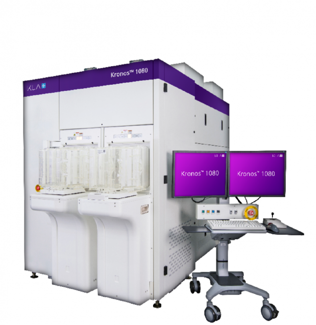
Kronos™ 1190
Kronos™ 1190
商品簡述:
The Kronos™ 1190 patterned wafer inspection system with high resolution optics provides best in class sensitivity to critical defects for process development and production monitoring in advanced wafer-level packaging (AWLP) applications including 3D IC and high-density fan-out (HDFO). DefectWise™ integrates Artificial Intelligence (AI) as a system level solution, delivering a large boost in sensitivity, productivity and classification accuracy to address the challenges of overkill and defect escapes. DesignWise™ refines the FlexPoint™ precisely targeted inspection areas with direct design input to further reduce nuisance. Supporting bonded, thinned, warped and diced substrates, the Kronos 1190 system enables cost-effective defect inspection down to 150nm in critical process steps like post-dicing, pre-bonding, patterning of Cu pads, Cu pillars, bumps, through silicon vias (TSVs) and redistribution layers (RDL).
Applications
Defect discovery, Process debug, Process monitor, Tool monitor, Outgoing Quality Control (OQC)
Related Products
CIRCL-AP : The Kronos inspection technology is also available as a module on the CIRCL defect inspection, metrology and review cluster tool.
更多產品資料 ......