1 /
1
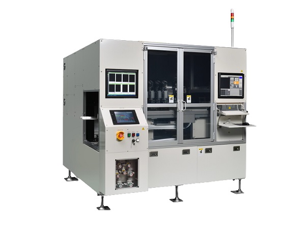
Plasma Laser Repair Equipment
ALR-04G-P4
ALR-04G-P4
商品简述:
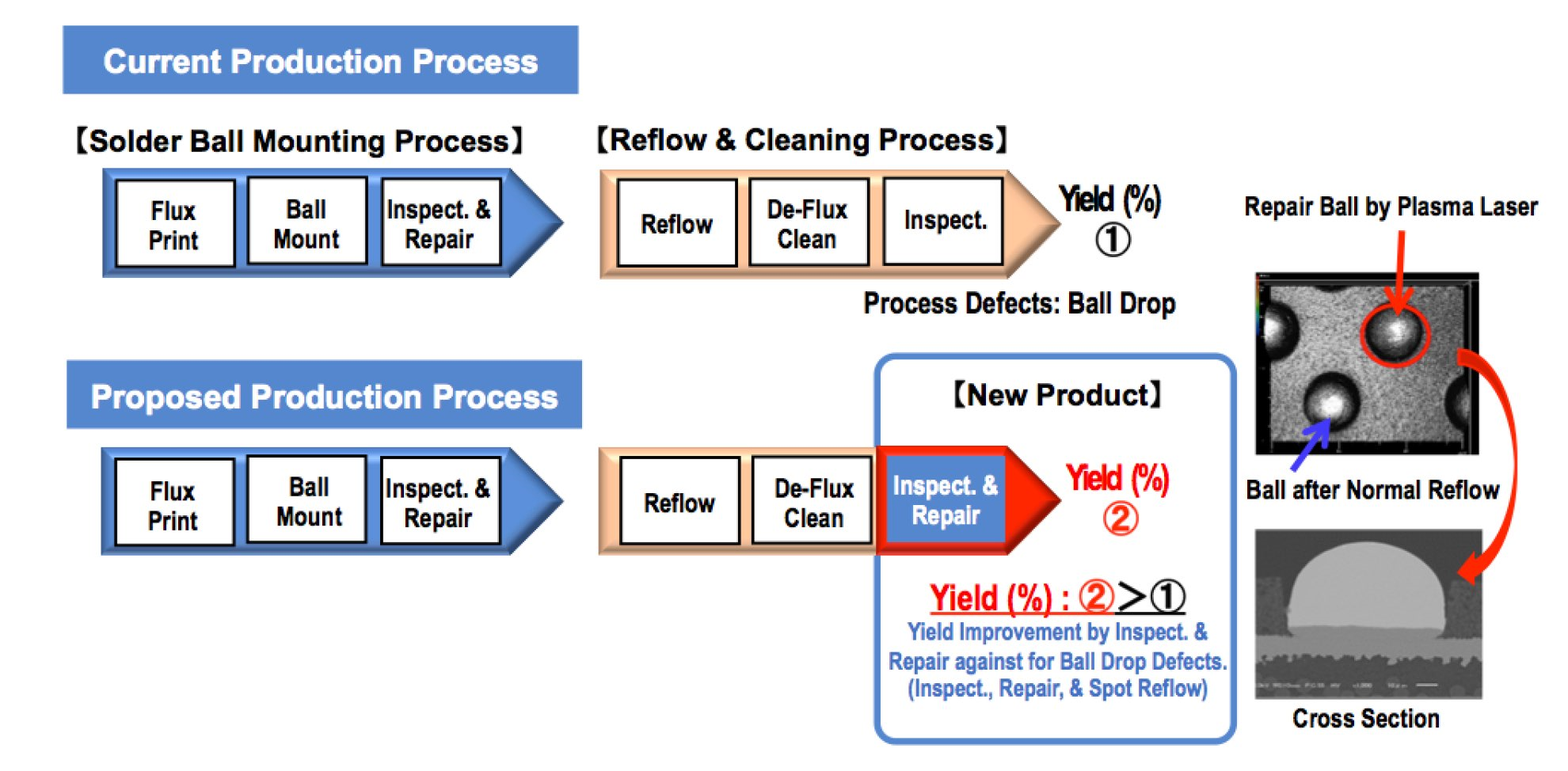
Plasma Laser Repair Equipment for Semiconductor Packages enabling Yield Improvement
- Enabled Inspection and Repair for Solder Ball Drop Defects during Reflow and De-Flux Cleaning Process after Ball Mounting
- Realized Spot Reflow soldering (local soldering for only repairing points) by integrating Plasma and Laser Technologies
- Minimized Reflow Process impacting qualities of Semiconductor Packages
- Realized Inspection & Repair for Ball Drop Defects during Reflow and Cleaning Process
- High Speed Overall Surface Inspection for Work(Substrate and Wafer)
- Flux dipping & High Precision Solder Ball Mounting
- Soldering by Plasma & Laser technologies
- Proposal for Off-Line or In-Line System
| No. | Items | Specifications |
|---|---|---|
| 1 | Work Size | Wafer : Max. 12“ (φ300mm) |
| 2 | Work Type | Wafer (WLCSP, FOWLP, etc.) |
| 3 | Applied Ball Diameter | 30um - 300um |
| 4 | Inspection Method | On the Fly Inspection |
| 5 | Solder Ball soldering Method | Plasma + Laser |
| 6 | Cycle Time (Repair + Solder Ball soldering) |
50 sec. |
| 7 | Equipment Dimensions | W2,600 x D2,400 x H2,150mm |
| 8 | Equipment Weight | 3,000 kg |