

1 /
1
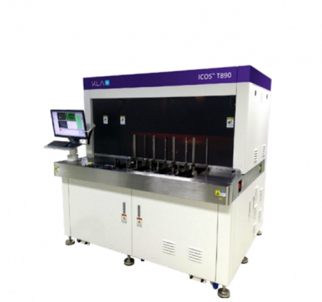
Packaged IC Inspection and Metrology Systems
ICOS™ T890
ICOS™ T890
Description:
Flexibility & Upgradability
A common platform is used for tools with tray and tape output. Upgrades from tray to tape and vice versa are available for optimal tool use in a changing environment. For customers looking for continuity, the ICOS™ 2CAM, 3CAM and aPVI solutions remain available in the T3 and T7 product family. Upgrades to later technologies are available should the requirements from the end customer change.
2D & 3D Metrology
BGA, CSP, SGA Balls and Solder Pads - The BGA/CSP ball inspection system inspects BGA and CSP devices for critical items such as coplanarity, ball presence, position, offset, pitch, extra ball, body width, ball damage and discolored balls.
Generic Shapes - With the latest SIGMA 3D metrology, it is possible to inspect generic features on the device such as passive components and surface dents.
LGA Lands - The LGA 3D measurement inspects the correctness of the LGA pad grid by measuring 2D and 3D items such as pad coplanarity, offset, pitch and width.
QFN Pads Lands - This application inspects QFN and other “leadless” packages. The system measures pad position, size, pitch, etc. In addition, it checks body size and edge straightness to control the sawing process.
QFP/SOP Leads - The Lead 3D application performs 3D inspection of all gull wing components. It can inspect for items such as lead coplanarity, offset, skew, pitch, length, width, span, sweep, slant, terminal dimension, body standoff and foot angle.
Top & Bottom Package Visual Inspection (PVI)
SPECTRUM+ or aPVI - This option offers state-of-the-art inspection of the package surface. It scans the device for voids, scratches, pits, packageincomplete fill, non-homogenous molding, foreign material, chips and similar defects. Due to its highly flexible illumination, a variety of surface materials can be inspected, including plastic mold, exposed silicon, metal surfaces, substrate, etc.
xCrack+™ - This option on SPECTRUM+ allows the detection of μcracks in silicon or mold.
Color Inspection - With this option, defects like discoloration on EMI shields, exposed wire bond copper, plating defects can be detected.
More......